- Low dimensional electronic and optoelectronic devices
- Quantum engineering
- Oxide Electronics
- Power Electronics
- Non-crystalline materials and devices
Research in the Micro and Nano-electronics is carried out at the level of the key “building blocks” of electronics, such as transistors, diodes, memristors, and memory cells. The field is at the intersection between physics, chemistry & materials science and circuits, architecture & systems. As such, the research combines fundamental and applied aspects, for example by leveraging unique properties of materials for certain applications and functions, or deepening the understanding of the principle of operation of devices by advanced characterization. The Faculty of Electrical and Computer Engineering at the Technion includes advanced micro-fabrication and characterization facilities, both at the micro-nano fabrication unit (MNFU) and at the principal investigators’ labs. The research is carried out in a wide range of topics, including organic materials devices (e.g. for transparent and flexible electronics), nano-materials and oxide electronics, logic and memory devices, power devices, quantum engineering devices, micro and nano electro mechanical systems (MEMS\NEMS), and more.
Read More
Low dimensional electronic and optoelectronic devices
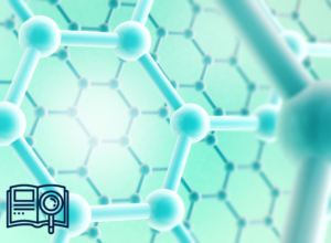
During the last few decades, semiconductor devices have been continuously scaled down to meet the ever-increasing demands for higher performance, operation speed, and lower power consumption. As devices approach fundamental scaling limits, low dimensional materials offer novel technological avenues and new paradigms for the development of advanced devices, functionalities, and applications with improved performance beyond state-of-the-art. Low dimensional materials are atomically thin 2D-sheets, 1D-wires, and 0D-dots, which exhibit unique electrical, optical, and thermal properties due to naturally confined electronic, phononic and photonic states of matter. The continuously improved quality of low-dimensional materials having naturally passivated surfaces without dangling bonds allow stacking these materials together, forming superior heterostructures as well as integrating them heterogeneously with conventional 3D-bulk materials (e.g., Silicon), overcoming the problems related to lattice-mismatch and interface defects. Immediate applications include low power transistors and memory elements with ultimate scaling, power-efficient optical interconnect, high-speed electro-optic modulators, advanced broadband photodetectors, thermal links and flexible/transparent (opto)electronics.
The group of Yuval Yaish studies both fundamental and applied aspects of the electrical and mechanical coupling between 1D (carbon nanotubes) and 2D materials for realizing electrical and quantum computing devices. Ilya Goykhman’s lab is focused on hybrid 2D-silicon photonics, plasmonics, heterostructures, and integrated optoelectronics. Eilam Yalon’s group studies energy-efficient electronics based on 2D materials, including transistors, memory elements, switches, and neuromorphic hardware building blocks. The research in all three groups includes design, nanofabrication, advanced characterization, and modeling of nano electronic and optoelectronic devices.
Quantum engineering
In this field of research quantum phenomena are employed for novel applications in metrology and in data processing. The group of Ido Kaminer studies quantum interaction between free electrons and light, and explores photonic quantum computing. Quantum electrodynamics, superconductor-semiconductor quantum optoelectronic devices, high-temperature superconductor-semiconductor optoelectronic devices, exciton–polariton ultrafast condensate dynamics, and 2D-material-based devices are studied by the group of Alex Hayat. The group of Eyal Buks develops an optical interface for superconducting quantum devices, and studies spins in diamond.
Oxide Electronics
Unlike the classical use of oxides as insulators in microelectronics, in our field we study unusual oxides as future semiconductors, as conductors with unique features, and as magnetic materials that will form future memories. This field brings together fundamental physics of oxides, their band structure, behaviour of electrons and spins, and engineering and understanding of new devices that leverage the unique properties of these materials. This is combined with advanced materials methods for synthesizing new materials with exotic properties and characterizing them on a sub-picometer scale. These approaches are brought together to design and develop advanced generations of electronic, memory and renewable energy devices, that harness the unique physics of oxides.
For more information contact Lior Kornblum, liork@ee.technion.ac.il
Power Electronics
Electrical cars, computers, solar energy systems, and any modern electrical and electronic equipment require sophisticated electronics for handling their power requirements. These circuits are composed of specialized devices, that differ fundamentally from standard digital transistors. In addition, wireless communication systems require components that can supply high power rates at microwave frequencies.
Here at Technion, we collaborate with industry and research institutes, by studying power devices using computer simulations. We study transistors made of a semiconductor called gallium nitride, which are better suited for power applications than silicon devices. We strive to understand their device physics and improve their performance.
For more information, please contact Prof. Dan Ritter.
Non-crystalline materials’-based devices (amorphous, printable, …)
The majority of the devices changing our lives are based on crystalline materials which are well defined and relatively known. Materials that are inherently disordered or even amorphous are, by definition, less defined and hence designing and fabricating devices could be frustrating. As a device engineer one has to often resorts to basic physics questions or more precisely chemical-physics questions, to build the knowledge, methods, and tools that exist in other fields. The range of materials addressed by the group of Nir Tessler include organic (sometime called plastic), inorganic (incl. nanocrystals), and hybrid organic-inorganic. The devices could be solar cells, transistors (incl. electro-chemical ones), diodes or even sensors (as in artificial nose).


